Hardware access: sys.gpio and sys.i2c
firmware, the same way sys.store/sys.fetch do: a C function in the
firmware’s natives.h, a thin wrapper in glue.c, an entry in the
generated stdlib table. Other backends (browser, sim, terminal, pure-js)
do not have them — check before calling, the way examples/gpio and
examples/i2c do:
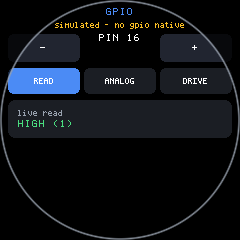
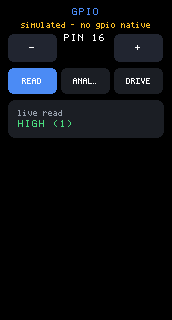
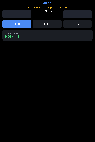
var HAVE = typeof sys !== 'undefined' && typeof sys.gpio === 'function';sys.gpio(pin, op, value) -> int
Section titled “sys.gpio(pin, op, value) -> int”| op | does | returns |
|---|---|---|
| 0 | read: INPUT_PULLUP, then digitalRead | 0 or 1 |
| 1 | write: OUTPUT, then digitalWrite(value) | 1 |
| 2 | analogRead | the ADC count |
Returns -1 for a refused pin or an unknown op.
Things to know:
- Reading reconfigures the pin. op 0 sets
INPUT_PULLUPevery call, so polling a pin you just drove releases it. An open pin reads 1, not 0 — that is the pullup. - The ADC does not reach every pin. On the ESP32-S3 only GPIO 1..20 are ADC-capable; op 2 elsewhere reads nothing useful.
sys.i2c(addr, reg, value) -> int
Section titled “sys.i2c(addr, reg, value) -> int”One byte of a device on the board’s shared I2C bus. value omitted or
negative reads (write reg, repeated-start, read one byte); value 0..255
writes that byte. Returns the byte read, 1 on a good write, -1 on no
answer or a bad address (accepted range 0x03..0x77). It is the same Wire
sequence as the bridge’s reg TCP command, which is the bring-up tool it
mirrors.
The bus is the one the touch controller lives on, and on some boards much more: the 3.5” board’s I/O expander, power-management chip, RTC, IMU and audio codec all share it. A read is usually harmless (though some devices clear interrupt flags on read); a stray register write to the PMU is not. Scan first, write only registers you know.
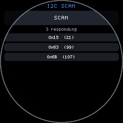
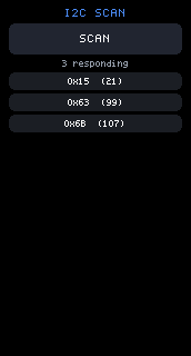
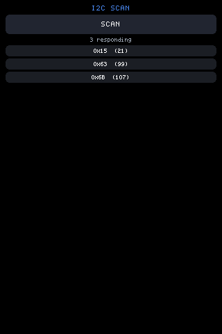
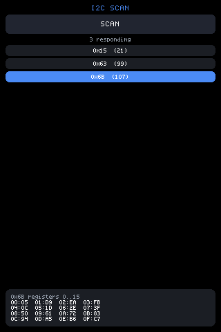
examples/i2c is that advice as a program: it walks 0x08..0x77 a few
addresses per tick so the UI stays live, lists what answered, and peeks
registers 0..15 of whichever address you tap.
Safety rules
Section titled “Safety rules”The firmware refuses, with -1, any sys.gpio pin the active board’s
display or touch controller uses — the denylist is built from the same
config.h defines that wire those peripherals, so it tracks the board the
build is for. A script poking the panel’s DC line mid-frame rewrites the
display’s command state; that class of accident is fenced off rather than
trusted away.
The denylist covers display and touch only. Reader UART pins are not refused — on a board with PN532s attached, driving those pins disturbs the readers.
Board pin notes
Section titled “Board pin notes”Refused pins (display + touch) and what else is spoken for, per board:
- 1.69” 240x280 (BOARD 1): refused 4, 5, 6, 7, 8, 15 (panel) and 10, 11, 13, 14 (touch). Reader UARTs sit on 17/18, 2/3 and 43/44.
- 3.5” 320x480 (BOARD 2): refused 1, 2, 3, 5, 6 (panel) and 7, 8 (the shared I2C bus). Readers on 44/43, 15/16, 13/14; SD on 9/10/11; the camera owns 17, 18, 21 and 38..48.
- 1.47” 172x320 (BOARD 3): refused 21, 38, 39, 40, 45, 46 (panel) and 41, 42, 47, 48 (touch). Reader UART on 43/44; 17/18 are SD data lines, not spare.
- round 1.28” 240x240 (BOARD 4): refused 2, 8, 9, 10, 11, 14 (panel) and 5, 6, 7, 13 (touch). The SH1.0 header brings out 15, 16, 17, 18, 21, 33; the single reader uses 17/18.
Not exposed: serial/UART
Section titled “Not exposed: serial/UART”There is no sys.uart. The board’s UARTs belong to the PN532 readers
today, routed through the GPIO matrix to the pins listed above, and a
script sharing them would corrupt reader frames. Exposing a UART on a
build that gives up a reader slot is future work.